

R&D and Trial Manufacturing Facility
Quantiam’s 34,000 ft2 R&D and trial manufacturing facility in Edmonton houses our extensive in-house materials characterization and development capabilities. Contact us today to find out how we can solve your materials and process-related pain points.
Materials Characterization
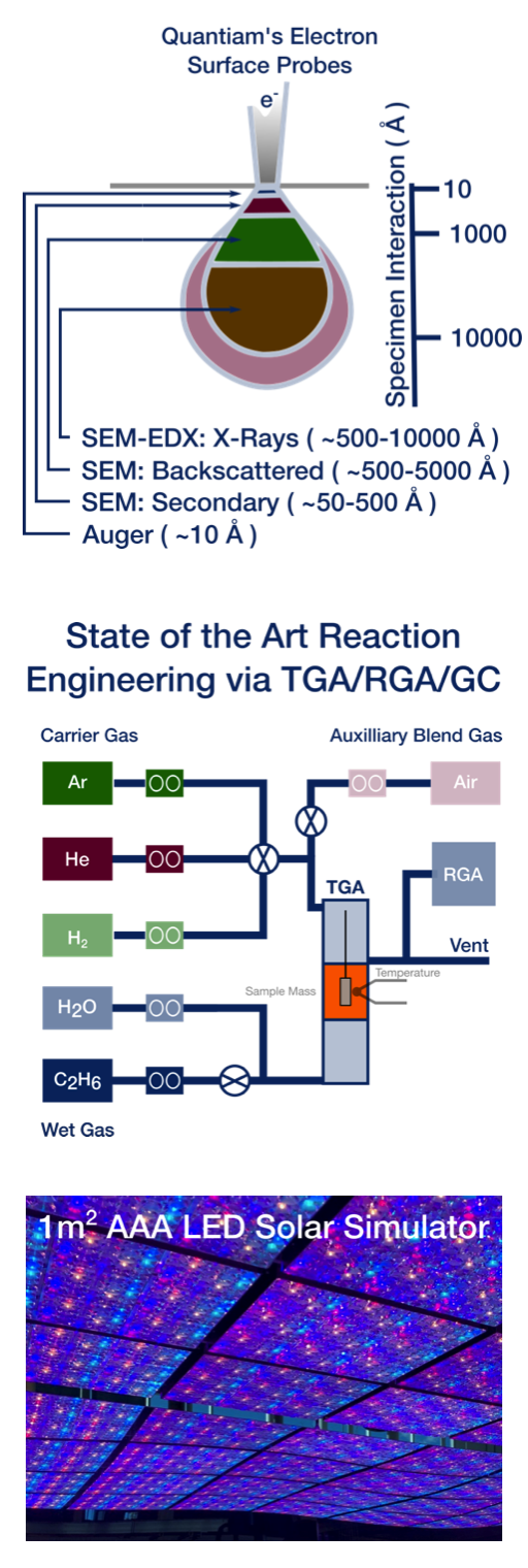
Surface and Advanced Structure Probes
- Two X-ray diffraction units, one for high temperature
- One FESEM-EDS and one SEM/EDS
- Auger Electron Spectroscopy (AES) with SIMS
- Small-spot X-Ray Photoelectron Spectroscopy (XPS)
Metallography
- Conventional and Damage-sensitive materials
- Hot and cold sample mounting
- Optical microscopy
Physical and Mechanical Properties
- Hardness testing (micro and macro)
- Instron Tensile and bend-testing
- Fracture toughness (pull and bend-testing)
- Surface roughness and optical profilometry
- 3D laser mapping for internal surfaces of tubulars
Particle/Powder Testing
- Particle size analysis (laser diffraction and DLS)
- Zeta potential
- BET surface area
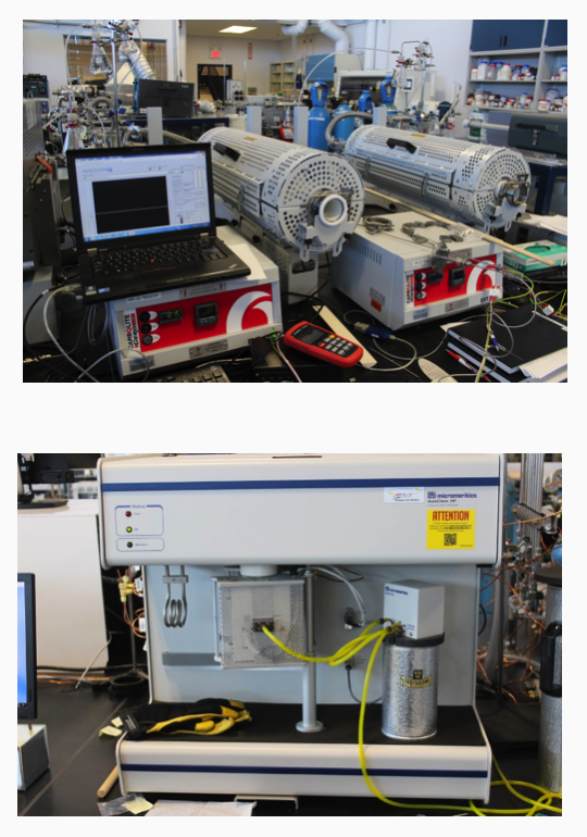
Thermogravimetric Analysis
- Three TGA units; powder and coupon samples to 35g
- Up to 1600°C
- Testing atmospheres include:
- up to 100% Hydrogen
- up to 90% steam/humidity
- Ethane-steam pyrolysis
- Oxidizing/inert/reducing/reactive gases
- Differential scanning calorimetry
Electrochemical Testing
- Keithley single channel potentiostat
- PARStat 8-channel potentiostat
- Arbin 32-channel potentiostat with Gamry EIS
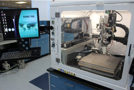
Photovoltaic Testing
- G2V AM1.5G solar simulators
- 400 cm2
- 1 m2
Materials Performance Testing
High Temperature Testing
Extensive high temperature testing up to 1500°C under various atmospheres including:
- Vacuum (< 10-3 Torr)
- Inert
- Oxidizing
- Reducing
- Carburizing
- Reactive gases
Wear Performance Testing
- ASTM G65 Abrasion Wear Testing
- ASTM G99 Pin-on-Disk Wear Testing
- ASTM G133 Sliding Wear Testing
- ASTM G17 Scratch Resistance Testing
Catalyst Testing
Catalyst performance testing/screening:
- temperatures up to 1000°C
- pressures up to 50 atm.
- on-line analysis of reaction products with gas chromatography (GC) and mass spectrometry (MS)
Materials, Manufacturing & Process Development
Rapid Prototyping
- OpenFoam CAD
- 3D printing
Coating Development
- Quantiam-proprietary coating manufacturing technology for internal and external surfaces of complex shapes.
- tape-casting to 25mm thickness
- spray coating:
- 2D Sono-tek spray coater with temperature control
- 3D 5-axis robot arm spray coater for full-scale workpieces
Powder Processing
- Ball-milling
- Mechanical alloying
- Lab-scale and production-scale attritors
Chemical Process Development
- Air-free chemical synthesis
- Modular jacketed reactor system for batch sizes of 100 mL – 5L
Surface Analysis Capabilities
| Technique Characteristics | JEOL JSM-7001F FE-SEM/EDS |
JEOL |
Perkin Elmers |
Perkin Elmers PHI-600 SAM/SIMS |
|
| Field Emission Scanning Electron Microscopy w/ Energy Dispersive Spectroscopy | Scanning Electron Microscopy w/ Energy Dispersive Spectroscopy | X-ray Photoelectron Spectroscopy (XPS) | Auger Electron Spectroscopy/ Scanning Auger Multiprobe (AES-SAM) |
Secondary Ion Mass Spectrometry (SIMS) | |
| Probe | electrons | electrons | x-ray | electrons | ions |
| Detected Particles | electrons and photons | electrons and photons | electrons | electrons | +ve or -ve ions |
| Range | B and higher | B and higher | Li and higher | Li and higher | 1 - 511 amu |
| Sampling Depth | 0.5 – 5 µm | 0.5 – 5 µm | 10 - 50 Å | 4 - 30 Å | 20 - 50 Å |
| Detection Limit* | 0.5 to 2.0 at% | 0.5 to 2.0 at% | 0.1 to 1.0 at% | 0.1 to 1.0 at% | ppm to ppb |
| Depth Profiling (Speed and Type) | N/A | N/A | fast, argon ions | fast, argon ions | fast, argon/oxygen |
| Information | elemental | elemental | elemental, chemical | elemental, some chemical | elemental, some structural |
| Quantitative | semi | semi | semi | semi | not usually |
| Probe Spatial Resolution | 1.2 nm | 4.0 nm | 75 µm | ~35 nm | 200 µm to 1 mm |
| Advantages |
excellent spatial resolution
elemental mapping
|
excellent spatial resolution
elemental mapping
|
few limitations on sample type
chemical state information
low damage to sample
|
good spatial resolution
elemental mapping
analyzing conductors and semiconductors |
excellent sensitivity
isotope and hydrogen detection
|
* Detection limit varies by element